


108,54 zł Netto

darmowa wysyłka na terenie Polski dla wszystkich zamówień powyżej 500 PLN

Jeśli Twoja wpłata zostanie zaksięgowana na naszym koncie do godz. 11:00

Każdy konsument może zwrócić zakupiony towar w ciągu 14 dni bez zbędnych pytań
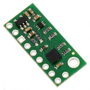
This sensor is a carrier/breakout board for the ST L3G4200D three-axis gyroscope, which measures the angular rates of rotation about the pitch (x), roll (y), and yaw (z) axes. Angular velocity measurements with a configurable range of ±250°/s, ±500°/s, or ±2000°/s can be read through a digital I2C or SPI interface. The board has a 3.3 V linear regulator and integrated level-shifters that allow it to work over an input voltage range of 2.5–5.5 V, and the 0.1” pin spacing making it easy to use with standard solderless breadboards and 0.1” perfboards.
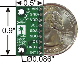 |
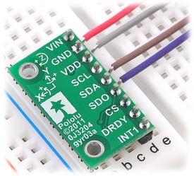
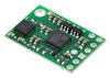
This board is a compact (0.5? ? 0.9?) breakout board for ST’s L3G4200D ultra-stable three-axis digital-output gyroscope; we therefore recommend careful reading of the L3G4200D datasheet (1MB pdf) before using this product. The L3G4200D is a great IC, but its small, leadless, LGA package makes it difficult for the typical student or hobbyist to use. It also operates at voltages below 3.6 V, which can make interfacing difficult for microcontrollers operating at 5 V. This carrier board addresses these issues by incorporating additional electronics, including a 3.3 V voltage regulator and level-shifting circuits, while keeping the overall size as compact as possible. The board ships fully populated with its SMD components, including the L3G4200D, as shown in the product picture.
The L3G4200D has many configurable options, including three selectable angular rate sensitivities, a choice of output data rates, an embedded FIFO for buffering output data, and a programmable external interrupt signal. The three angular velocity readings are available through a digital interface, which can be configured to operate in either I˛C or SPI mode.
The carrier board includes a low-dropout linear voltage regulator that provides the 3.3 V required by the L3G4200D, which allows the sensor to be powered from a 2.5-5.5 V supply. The regulator output is available on the VDD pin and can supply almost 150 mA to external devices. The breakout board also includes a circuit that shifts the I˛C/SPI clock and data in lines to the same logic voltage level as the supplied VIN, making it simple to interface the board with 5 V systems, and the board’s 0.1? pin spacing makes it easy to use with standard solderless breadboards and 0.1? perfboards.
For sensor fusion applications, our MinIMU-9 inertial measurement unit combines the L3G4200D with an LSM303DLH 3-axis accelerometer and 3-axis magnetometer on a board barely bigger than this L3G4200D carrier alone, providing nine independent readings that can be used to calculate an absolute orientation.
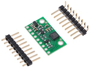
A 9?1 strip of 0.1? header pins and a 9?1 strip of 0.1? right-angle header pins are included, as shown in the picture below. You can solder the header strip of your choice to the board for use with custom cables or solderless breadboards, or you can solder wires directly to the board itself for more compact installations.
 |
Regardless of the interface being used to communicate with the L3G4200D, its VIN pin should be connected to a 2.5-5.5 V source, and GND should be connected to 0 volts. (Alternatively, if you are using the gyro with a 3.3 V system, you can leave VIN disconnected and bypass the built-in regulator by connecting 3.3 V directly to VDD.)
A minimum of two logic connections are necessary to use the L3G4200D in I˛C mode (this is the default mode): SCL and SDA. These should be connected to an I˛C bus operating at the same logic level as VIN.
To use the L3G4200D in SPI mode, four logic connections are required: SPC, SDI, SDO, and CS. These should be connected to an SPI bus operating at the same logic level as VIN. The SPI interface operates in 4-wire mode by default, with SDI and SDO on separate pins, but it can be configured to use 3-wire mode so that SDO shares a pin with SDI.
|
|
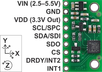
| PIN | Description |
|---|---|
| VIN | This is the main 2.5-5.5 V power supply connection. The SCL/SPC and SDA/SDI level shifters pull the I˛C and SPI bus high bits up to this level. |
| GND | The ground (0 V) connection for your power supply. Your I˛C or SPI control source must also share a common ground with this board. |
| VDD | Regulated 3.3 V output. Almost 150 mA is available to power external components. (If you want to bypass the internal regulator, you can instead use this pin as a 3.3 V input with VIN disconnected.) |
| SCL/SPC | Level-shifted I˛C/SPI clock line: HIGH is VIN, LOW is 0 V |
| SDA/SDI | Level-shifted I˛C data line and SPI data in line (also doubles as SDO in 3-wire mode): HIGH is VIN, LOW is 0 V |
| SDO | SPI data out line in 4-wire mode: HIGH is VDD, LOW is 0 V. This output is not level-shifted. Also used as an input to determine I˛C slave address (see below). |
| CS | SPI enable (chip select). Pulled up to VDD to enable I˛C communication by default; drive low to begin SPI communication. |
| DRDY/INT2 | Data ready indicator, a 3.3-V-logic-level output. HIGH (3.3 V) indicates angular rate data can be read. Can also be configured as a FIFO interrupt. This output is not level-shifted. |
| INT1 | Programmable interrupt, a 3.3-V-logic-level output. This output is not level-shifted. |
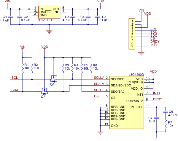 |
The above schematic shows the additional components the carrier board incorporates to make the L3G4200D easier to use, including the voltage regulator that allow the board to be powered from a 2.5-5.5 V supply and the level-shifter circuit that allows for I˛C and SPI communication at the same logic voltage level as VIN.
With the CS pin in its default state (pulled up to VDD), the L3G4200D can be configured and its angular velocity readings can be queried through the I˛C bus. Level shifters on the I˛C clock (SCL) and data (SDA) lines enable I˛C communication with microcontrollers operating at the same voltage as VIN (2.5-5.5 V). A detailed explanation of the I˛C interface on the L3G4200D can be found in its datasheet (1MB pdf), and more detailed information about I˛C in general can be found in NXP’s I˛C-bus specification (371k pdf).
In I˛C mode, the gyro’s 7-bit slave address has its least significant bit (LSb) determined by the voltage on the SDO pin. The carrier board pulls SDO to VDD through a 10 kΩ resistor, making the LSb 1 and setting the slave address to 1101001b by default. If the gyro’s selected slave address happens to conflict with some other device on your I˛C bus, you can drive SDO low to set the LSb to 0.
In our tests of the board, we were able to communicate with the chip at clock frequencies up to 400 kHz; higher frequencies might work but were not tested. The chip itself and carrier board do not meet of some requirements to make the device compliant with I˛C fast-mode. It is missing 50 ns spike suppression on the clock and data lines, and additional pull-ups on the clock and data lines might also be necessary to achieve compliant signal timing characteristics.
To communicate with the L3G4200D in SPI mode, the CS pin (which the board pulls to VDD through a 10 kΩ resistor) must be driven low before the start of an SPI command and allowed to return high after the end of the command. Level shifters on the SPI clock (SPC) and data in (SDI) lines enable SPI communication with microcontrollers operating at the same voltage as VIN (2.5-5.5 V).
In the default 4-wire mode, the gyro transmits data to the SPI master on a dedicated data out (SDO) line. If the SPI interface is configured to use 3-wire mode instead, the SDI line doubles as SDO and is driven by the L3G4200D when it transmits data to the master. A detailed explanation of the SPI interface on the L3G4200D can be found in its datasheet (1MB pdf).
We have written a basic Arduino library for the L3G4200D that makes it easy to interface this sensor with an Arduino. The library makes it simple to configure the L3G4200D and read the raw gyro data through I˛C.
The datasheet provides all the information you need to use this sensor, but picking out the important details can take some time. Here are some pointers for communicating with and configuring the L3G4200D that we hope will get you up and running a little bit faster:
 |
MinIMU-9 Gyro, Accelerometer, and Compass (L3G4200D and LSM303DLM Carrier) |
 |
MMA7341L 3-Axis Accelerometer ±3/11g |
 |
MMA7341L 3-Axis Accelerometer ±3/11g with Voltage Regulator |
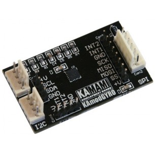
Moduł 3-osiowego żyroskopu z układem L3G4200D, wyposażony w interfejsy I2C i SPI. Zasilanie napięciem 3..5 V, w komplecie złącza 2,54 mm proste i kątowe. GY-50
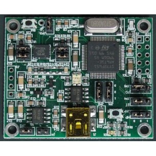
PmodGYRO, moduł z 3-osiowym żyroskopem L3G4200D, SPI, I2C, 800 Hz. Digilent 410-215
Brak towaru
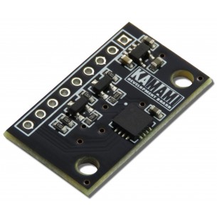
Moduł z układem L3G4200D (3-osiowy żyroskop z wyjściem cyfrowym)
Prosty w użyciu moduł z 3-osiowym żyroskopem L3GD20, interfejs I2C lub SPI, zasilanie 2.5..5.5V, regulator napięcia wyjściowego 3.3V, regulowany szerszy zakres czułości ±245°/s, ±500°/s, lub ±2000°/s, kompatybilny z Arduino i Raspberry Pi. Pololu 2129
KAmodL3GD20 to moduł żyroskopu cyfrowego z układem L3GD20. Pozwala na pomiar prędkości kątowej do ±2000 stopni na sekundę. KAmodL3GD20
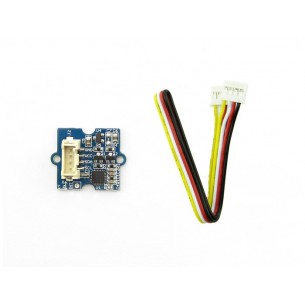
Moduł z 3-osiowym żyroskopem (układ ITG 3200). Zakres pomiarowy wynosi ±2000°/s. Do komunikacji wykorzystywany jest interfejs I2C. Moduł cechuje się niewielkim poborem prądu (typowo 6,5 mA) Moduł posiada złącze zgodne z standardem Grove. Seeed studio 101020050